Conventional PCI
Conventional PCI, often shortened to PCI, is alocal computer bus for attaching hardware devices in a computer. PCI is the initialism forPeripheral Component Interconnect[2] and is part of the PCI Local Bus standard. The PCI bus supports the functions found on aprocessor bus but in a standardized format that is independent of any particular processor's native bus. Devices connected to the PCI bus appear to a bus master to be connected directly to its own bus and are assigned addresses in the processor'saddress space[3]. It is a parallel bus, synchronous to a single bus clock.
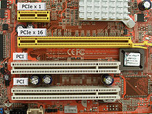
Attached devices can take either the form of an integrated circuit fitted onto the motherboard itself (called a planar device in the PCI specification) or an expansion cardthat fits into a slot. The PCI Local Bus was first implemented in IBM PC compatibles, where it displaced the combination of several slow ISA slots and one fast VESA Local Busslot as the bus configuration. It has subsequently been adopted for other computer types. Typical PCI cards used in PCs include: network cards, sound cards,modems, extra ports such as USB or serial, TV tuner cards and disk controllers. PCI video cards replaced ISA and VESA cards until growing bandwidth requirements outgrew the capabilities of PCI. The preferred interface for video cards then became AGP, itself a superset of conventional PCI, before giving way to PCI Express.[4]
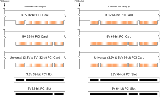
The first version of conventional PCI found in consumer desktop computers was a 32-bitbus using a 33 MHz bus clock and 5 V signalling, although the PCI 1.0 standard provided for a 64-bit variant as well. These have one locating notch in the card. Version 2.0 of the PCI standard introduced 3.3 V slots, physically distinguished by a flipped physical connector to prevent accidental insertion of 5 V cards. Universal cards, which can operate on either voltage, have two notches. Version 2.1 of the PCI standard introduced optional 66 MHz operation. A server-oriented variant of conventional PCI, called PCI-X (PCI Extended) operated at frequencies up to 133 MHz for PCI-X 1.0 and up to 533 MHz for PCI-X 2.0. An internal connector for laptop cards, calledMini PCI, was introduced in version 2.2 of the PCI specification. The PCI bus was also adopted for an external laptop connector standard – the CardBus.[5] The first PCI specification was developed by Intel, but subsequent development of the standard became the responsibility of the PCI Special Interest Group (PCI-SIG).[6]
Conventional PCI and PCI-X are sometimes called Parallel PCI in order to distinguish them technologically from their more recent successor PCI Express, which adopted a serial, lane-based architecture.[7][8]Conventional PCI's heyday in the desktop computer market was approximately 1995–2005.[7] PCI and PCI-X have become obsolete for most purposes; however, they are still common on modern desktops for the purposes of backwards compatibility and the low relative cost to produce. Many kinds of devices previously available on PCI expansion cards are now commonly integrated onto motherboards or available in USB and PCI Express versions.
History
Work on PCI began at Intel's Architecture Development Lab c. 1990. A team of Intel engineers (composed primarily of ADL engineers) defined the architecture and developed a proof of concept chipset and platform (Saturn) partnering with teams in the company's desktop PC systems and core logic product organizations.
PCI was immediately put to use in servers, replacing MCA and EISA as the server expansion bus of choice. In mainstream PCs, PCI was slower to replace VESA Local Bus(VLB), and did not gain significant market penetration until late 1994 in second-generation Pentium PCs. By 1996, VLB was all but extinct, and manufacturers had adopted PCI even for 486 computers.[9] EISA continued to be used alongside PCI through 2000. Apple Computer adopted PCI for professional Power Macintosh computers (replacing NuBus) in mid-1995, and the consumer Performaproduct line (replacing LC PDS) in mid-1996.
The 64-bit version of plain PCI remained rare in practice though,[10] although it was used for example by all (post-iMac) G3 and G4 Power Macintosh computers.[11]
Later revisions of PCI added new features and performance improvements, including a 66 MHz 3.3 V standard and 133 MHz PCI-X, and the adaptation of PCI signaling to other form factors. Both PCI-X 1.0b and PCI-X 2.0 are backward compatible with some PCI standards.
The PCI-SIG introduced the serial PCI Expressin c. 2004. At the same time, they renamedPCI as Conventional PCI. Since then, motherboard manufacturers have included progressively fewer Conventional PCI slots in favor of the new standard. Many new motherboards do not provide conventional PCI slots at all, as of late 2013.
Auto configuration
PCI provides separate memory and I/O portaddress spaces for the x86 processor family,64 and 32 bits, respectively. Addresses in these address spaces are assigned by software. A third address space, called thePCI Configuration Space, which uses a fixed addressing scheme, allows software to determine the amount of memory and I/O address space needed by each device. Each device can request up to six areas of memory space or I/O port space via its configuration space registers.
In a typical system, the firmware (or operating system) queries all PCI buses at startup time (via PCI Configuration Space) to find out what devices are present and what system resources (memory space, I/O space, interrupt lines, etc.) each needs. It then allocates the resources and tells each device what its allocation is.
The PCI configuration space also contains a small amount of device type information, which helps an operating system choose device drivers for it, or at least to have a dialogue with a user about the system configuration.
Devices may have an on-board ROMcontaining executable code for x86 or PA-RISC processors, an Open Firmware driver, or an EFI driver. These are typically necessary for devices used during system startup, before device drivers are loaded by the operating system.
In addition, there are PCI Latency Timers that are a mechanism for PCI Bus-Masteringdevices to share the PCI bus fairly. "Fair" in this case means that devices will not use such a large portion of the available PCI bus bandwidth that other devices are not able to get needed work done. Note, this does not apply to PCI Express.
Interrupts
Devices are required to follow a protocol so that the interrupt lines can be shared. The PCI bus includes four interrupt lines, all of which are available to each device. However, they are not wired in parallel as are the other PCI bus lines. The positions of the interrupt lines rotate between slots, so what appears to one device as the INTA# line is INTB# to the next and INTC# to the one after that. Single-function devices use their INTA# for interrupt signaling, so the device load is spread fairly evenly across the four available interrupt lines. This alleviates a common problem with sharing interrupts.
The mapping of PCI interrupt lines onto system interrupt lines, through the PCI host bridge, is implementation-dependent. Platform-specific BIOS code is meant to know this, and set the "interrupt line" field in each device's configuration space indicating which IRQ it is connected to.
PCI interrupt lines are level-triggered. This was chosen over edge-triggering in order to gain an advantage when servicing a shared interrupt line, and for robustness: edge triggered interrupts are easy to miss.
Later revisions of the PCI specification add support for message-signaled interrupts. In this system, a device signals its need for service by performing a memory write, rather than by asserting a dedicated line. This alleviates the problem of scarcity of interrupt lines. Even if interrupt vectors are still shared, it does not suffer the sharing problems of level-triggered interrupts. It also resolves the routing problem, because the memory write is not unpredictably modified between device and host. Finally, because the message signaling is in-band, it resolves some synchronization problems that can occur with posted writes and out-of-band interrupt lines.
PCI Express does not have physical interrupt lines at all. It uses message-signaled interrupts exclusively.
Conventional hardware specifications
These specifications represent the most common version of PCI used in normal PCs:
- 33.33 MHz clock with synchronoustransfers
- Peak transfer rate of 133 MB/s (133megabytes per second) for 32-bit bus width (33.33 MHz × 32 bits ÷ 8 bits/byte = 133 MB/s)
- 32-bit bus width
- 32- or 64-bit memory address space (4 gigabytes or 16 exabytes)
- 32-bit I/O port space
- 256-byte (per device) configuration space
- 5-volt signaling
- Reflected-wave switching
The PCI specification also provides options for 3.3 V signaling, 64-bit bus width, and 66 MHz clocking, but these are not commonly encountered outside of PCI-X support on server motherboards.
The PCI bus arbiter performs bus arbitration among multiple masters on the PCI bus. Any number of bus masters can reside on the PCI bus, as well as requests for the bus. One pair of request and grant signals is dedicated to each bus master.
Card voltage and keying
Typical PCI cards have either one or two key notches, depending on their signaling voltage. Cards requiring 3.3 volts have a notch 56.21 mm from the card backplate; those requiring 5 volts have a notch 104.47 mm from the backplate. "Universal cards" accepting either voltage have both key notches. This allows cards to be fitted only into slots with a voltage they support.
Connector pinout
The PCI connector is defined as having 62 contacts on each side of the edge connector, but two or four of them are replaced by key notches, so a card has 60 or 58 contacts on each side. Pin 1 is closest to the backplate. B and A sides are as follows, looking down into the motherboard connector.[13][15][16]
64-bit PCI extends this by an additional 32 contacts on each side which provide AD[63:32], C/BE[7:4]#, the PAR64 parity signal, and a number of power and ground pins.
Most lines are connected to each slot in parallel. The exceptions are:
- Each slot has its own REQ# output to, and GNT# input from the motherboard arbiter.
- Each slot has its own IDSEL line, usually connected to a specific AD line.
- TDO is daisy-chained to the following slot's TDI. Cards without JTAG support must connect TDI to TDO so as not to break the chain.
- PRSNT1# and PRSNT2# for each slot have their own pull-up resistors on the motherboard. The motherboard may (but does not have to) sense these pins to determine the presence of PCI cards and their power requirements.
- REQ64# and ACK64# are individually pulled up on 32-bit only slots.
- The interrupt lines INTA# through INTD# are connected to all slots in different orders. (INTA# on one slot is INTB# on the next and INTC# on the one after that.)
Notes:
- IOPWR is +3.3 V or +5 V, depending on the backplane. The slots also have a ridge in one of two places which prevents insertion of cards that do not have the corresponding key notch, indicating support for that voltage standard. Universal cards have both key notches and use IOPWR to determine their I/O signal levels.
- The PCI SIG strongly encourages 3.3 V PCI signaling,[13] requiring support for it since standard revision 2.3,[15] but most PC motherboards use the 5 V variant. Thus, while many currently available PCI cards support both, and have two key notches to indicate that, there are still a large number of 5 V-only cards on the market.
- The M66EN pin is an additional ground on 5 V PCI buses found in most PC motherboards. Cards and motherboards that do not support 66 MHz operation also ground this pin. If all participants support 66 MHz operation, a pull-up resistor on the motherboard raises this signal high and 66 MHz operation is enabled. The pin is still connected to ground via coupling capacitors on each card to preserve its ACshielding function.
- The PCIXCAP pin is an additional ground on conventional PCI buses and cards. If all cards and the motherboard support the PCI-X protocol, a pull-up resistor on the motherboard raises this signal high and PCI-X operation is enabled. The pin is still connected to ground via coupling capacitors on each card to preserve its AC shielding function.
- At least one of PRSNT1# and PRSNT2# must be grounded by the card. The combination chosen indicates the total power requirements of the card (25 W, 15 W, or 7.5 W).
- SBO# and SDONE are signals from a cache controller to the current target. They are not initiator outputs, but are colored that way because they are target inputs.
- PME# (19A) - Power management event (optional) which is supported in PCIversion 2.2 and higher. It is a 3.3 V, open drain, active low signal.[17] PCI cards may use this signal to send and receive PME via the PCI socket directly, which eliminates the need for a special Wake-on-LAN cable.[18]
Mixing of 32-bit and 64-bit PCI cards in different width slots
Most 32-bit PCI cards will function properly in 64-bit PCI-X slots, but the bus clock rate will be limited to the clock frequency of the slowest card, an inherent limitation of PCI's shared bus topology. For example, when a PCI 2.3, 66-MHz peripheral is installed into a PCI-X bus capable of 133 MHz, the entire bus backplane will be limited to 66 MHz. To get around this limitation, many motherboards have multiple PCI/PCI-X buses, with one bus intended for use with high-speed PCI-X peripherals, and the other bus intended for general-purpose peripherals.
Many 64-bit PCI-X cards are designed to work in 32-bit mode if inserted in shorter 32-bit connectors, with some loss of performance.[19][20] An example of this is the Adaptec 29160 64-bit SCSI interface card.[21]However, some 64-bit PCI-X cards do not work in standard 32-bit PCI slots.[22]
Installing a 64-bit PCI-X card in a 32-bit slot will leave the 64-bit portion of the card edge connector not connected and overhanging. This requires that there be no motherboard components positioned so as to mechanically obstruct the overhanging portion of the card edge connector.
Physical card dimensions
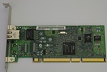
The maximum width of a PCI card is 15.24 mm (0.6 inches). Two bracket heights have been specified, known as full-height and low-profile. The bracket or backplate is the part that fastens to the card cage to stabilize the card. It also usually contains external connectors, so it attaches in a window in the computer case so any connectors are accessible from outside. The backplate is typically fixed to the case by either a 6-32 or M3 screw, or with a separate hold-down bracket that is part of the case.
For each bracket height two different lengths have been specified for a total of four lengths, known as full-length and half-length for full-height cards, and MD1 and MD2 for low-profile cards.
Full-height cards
The original full-height cards are defined by a bracket height of 120 mm (4.7 inches). The height of a full-height cards itself is nominally 107 mm (4.2 inches). The height includes the card edge connector.
Two lengths have been defined for full-height cards, known as full-length and half-length.
Full-length full-height card
The original full-length full-height PCI card (also known as full-size) is specified as a length of 312 mm (12.283 inches) and a height of 107 mm (4.2 inches). However, most modern PCI cards are half-length or smaller (see below) and many modern PC cases cannot accommodate the length of a full-size card. Note, this length is the length of the printed circuit board; it does not include the angled short leg of the metal bracket (which does affect e.g. packaging dimensions). Some high power PCI products have active cooling systems that extend past the nominal dimensions. Likewise, some may take up more than one slot space: these are referred to as double-wide or triple-wide cards, accordingly.
Half-length full-height card
A half-length full-height card has a length of up to 175.26 mm (6.9 inches) and a height of up to 107 mm (4.2 inches). The actual dimensions of many cards described as half-length full-height are lower than these maximums and they will still fit any standard full-height PCI slot as long as they use a properly located full-height bracket.
This is in fact the practical (de facto) standard now – the majority of modern PCI cards fit inside this envelope.
Low-profile cards
Low-profile PCI cards (also known as LPPCI or half-height cards) are defined by a bracket reduced in height to 79.2 mm (3.118 inches). The low-profile specification assumes a 3.3 volt PCI slot. The retention screw has also been moved 1.35 mm closer to the fold in the bracket.
The low profile card itself has a maximum height of 64.41 mm (2.536 inches) including the edge connector.
The smaller bracket will not fit a standard desktop, tower or 3U rack-mount PC case, but will fit in many newer small form-factor (SFF) desktop cases or in a 2U rack-mount case. These cards may be known by other names such as "slim".[23][24]
Many manufacturers supply both types of bracket with cards, where the bracket is typically attached to the card with a pair of screws allowing the installer to easily change it.
The PCI-SIG has defined two standard lengths for low-profile cards, known as MD1 and MD2.
MD1 low-profile card
MD1 defines the shortest 32-bit PCI card length, 119.91 mm (4.721 inches) and a maximum height of 64.41 mm (2.536 inches).
MD2 low-profile card
MD2 defines the maximum length of a low profile PCI card as 167.64 mm (6.600 inches) and a maximum height of 64.41 mm (2.536 inches). Any low profile PCI card longer than the MD1 length is considered an MD2 card. This is the most common low-profile card form-factor.
Beside conventional PCI, many PCI Expresscards are also described as MD2 low-profile form-factor.
Mini PCI
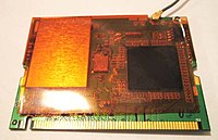
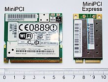
Mini PCI was added to PCI version 2.2 for use in laptops; it uses a 32-bit, 33 MHz bus with powered connections (3.3 V only; 5 V is limited to 100 mA) and support for bus mastering and DMA. The standard size for Mini PCI cards is approximately a quarter of their full-sized counterparts. There is no access to the card from outside the case, unlike desktop PCI cards with brackets carrying connectors. This limits the kinds of functions a Mini PCI card can perform.
Many Mini PCI devices were developed such as Wi-Fi, Fast Ethernet, Bluetooth, modems(often Winmodems), sound cards,cryptographic accelerators, SCSI, IDE–ATA,SATA controllers and combination cards. Mini PCI cards can be used with regular PCI-equipped hardware, using Mini PCI-to-PCIconverters. Mini PCI has been superseded by the much narrower PCI Express Mini Card.
Technical details of Mini PCI
Mini PCI cards have a 2 W maximum power consumption, which limits the functionality that can be implemented in this form factor. They also are required to support the CLKRUN# PCI signal used to start and stop the PCI clock for power management purposes.
There are three card form factors: Type I, Type II, and Type III cards. The card connector used for each type include: Type I and II use a 100-pin stacking connector, while Type III uses a 124-pin edge connector, i.e. the connector for Types I and II differs from that for Type III, where the connector is on the edge of a card, like with a SO-DIMM. The additional 24 pins provide the extra signals required to route I/O back through the system connector (audio, AC-Link, LAN, phone-line interface). Type II cards have RJ11 and RJ45 mounted connectors. These cards must be located at the edge of the computer or docking station so that the RJ11 and RJ45 ports can be mounted for external access.
Mini PCI is distinct from 144-pin Micro PCI.[25]
PC/104-Plus and PCI-104
Other physical variations
Typically consumer systems specify "N × PCI slots" without specifying actual dimensions of the space available. In some small-form-factor systems, this may not be sufficient to allow even "half-length" PCI cards to fit. Despite this limitation, these systems are still useful because many modern PCI cards are considerably smaller than half-length.
PCI bus transactions
PCI bus traffic consists of a series of PCI bus transactions. Each transaction consists of anaddress phase followed by one or more data phases. The direction of the data phases may be from initiator to target (write transaction) or vice versa (read transaction), but all of the data phases must be in the same direction. Either party may pause or halt the data phases at any point. (One common example is a low-performance PCI device that does not support burst transactions, and always halts a transaction after the first data phase.)
Any PCI device may initiate a transaction. First, it must request permission from a PCI bus arbiter on the motherboard. The arbiter grants permission to one of the requesting devices. The initiator begins the address phase by broadcasting a 32-bit address plus a4-bit command code, then waits for a target to respond. All other devices examine this address and one of them responds a few cycles later.
64-bit addressing is done using a two-stage address phase. The initiator broadcasts the low 32 address bits, accompanied by a special "dual address cycle" command code. Devices which do not support 64-bit addressing can simply not respond to that command code. The next cycle, the initiator transmits the high 32 address bits, plus the real command code. The transaction operates identically from that point on. To ensure compatibility with 32-bit PCI devices, it is forbidden to use a dual address cycle if not necessary, i.e. if the high-order address bits are all zero.
While the PCI bus transfers 32 bits per data phase, the initiator transmits 4 active-low byte enable signals indicating which 8-bit bytes are to be considered significant. In particular, a write must affect only the enabled bytes in the target PCI device. They are of little importance for memory reads, but I/O reads might have side effects. The PCI standard explicitly allows a data phase with no bytes enabled, which must behave as a no-op.
PCI address spaces
PCI has three address spaces: memory, I/O address, and configuration.
Memory addresses are 32 bits (optionally 64 bits) in size, support caching and can be burst transactions.
I/O addresses are for compatibility with the Intel x86 architecture's I/O port address space. Although the PCI bus specification allows burst transactions in any address space, most devices only support it for memory addresses and not I/O.
Finally, PCI configuration space provides access to 256 bytes of special configuration registers per PCI device. Each PCI slot gets its own configuration space address range. The registers are used to configure devices memory and I/O address ranges they should respond to from transaction initiators. When a computer is first turned on, all PCI devices respond only to their configuration space accesses. The computer's BIOS scans for devices and assigns Memory and I/O address ranges to them.
If an address is not claimed by any device, the transaction initiator's address phase will time out causing the initiator to abort the operation. In case of reads, it is customary to supply all-ones for the read data value (0xFFFFFFFF) in this case. PCI devices therefore generally attempt to avoid using the all-ones value in important status registers, so that such an error can be easily detected by software.
PCI command codes
There are 16 possible 4-bit command codes, and 12 of them are assigned. With the exception of the unique dual address cycle, the least significant bit of the command code indicates whether the following data phases are a read (data sent from target to initiator) or a write (data sent from an initiator to target). PCI targets must examine the command code as well as the address and not respond to address phases which specify an unsupported command code.
The commands that refer to cache lines depend on the PCI configuration space cache line size register being set up properly; they may not be used until that has been done.
- 0000: Interrupt Acknowledge
- This is a special form of read cycle implicitly addressed to the interrupt controller, which returns an interrupt vector. The 32-bit address field is ignored. One possible implementation is to generate an interrupt acknowledge cycle on an ISA bus using a PCI/ISA bus bridge. This command is for IBM PC compatibility; if there is noIntel 8259 style interrupt controller on the PCI bus, this cycle need never be used.
- 0001: Special Cycle
- This cycle is a special broadcast write of system events that PCI card may be interested in. The address field of a special cycle is ignored, but it is followed by a data phase containing a payload message. The currently defined messages announce that the processor is stopping for some reason (e.g. to save power). No device ever responds to this cycle; it is always terminated with a master abort after leaving the data on the bus for at least 4 cycles.
- 0010: I/O Read
- This performs a read from I/O space. All 32 bits of the read address are provided, so that a device may (for compatibility reasons) implement less than 4 bytes worth of I/O registers. If the byte enables request data not within the address range supported by the PCI device (e.g. a 4-byte read from a device which only supports 2 bytes of I/O address space), it must be terminated with a target abort. Multiple data cycles are permitted, using linear (simple incrementing) burst ordering.
- The PCI standard is discouraging the use of I/O space in new devices, preferring that as much as possible be done through main memory mapping.
- 0011: I/O Write
- This performs a write to I/O space.
- 010x: Reserved
- A PCI device must not respond to an address cycle with these command codes.
- 0110: Memory Read
- This performs a read cycle from memory space. Because the smallest memory space a PCI device is permitted to implement is 16 bytes,[15][13]:§6.5.2.1 the two least significant bits of the address are not needed during the address phase; equivalent information will arrive during the data phases in the form of byte select signals. They instead specify the order in which burst data must be returned.[15][13]:§3.2.2.2 If a device does not support the requested order, it must provide the first word and then disconnect.
- If a memory space is marked as "prefetchable", then the target device must ignore the byte select signals on a memory read and always return 32 valid bits.
- 0111: Memory Write
- This operates similarly to a memory read. The byte select signals are more important in a write, as unselected bytes must not be written to memory.
- Generally, PCI writes are faster than PCI reads, because a device may buffer the incoming write data and release the bus faster. For a read, it must delay the data phase until the data has been fetched.
- 100x: Reserved
- A PCI device must not respond to an address cycle with these command codes.
- 1010: Configuration Read
- This is similar to an I/O read, but reads from PCI configuration space. A device must respond only if the low 11 bits of the address specify a function and register that it implements, and if the special IDSEL signal is asserted. It must ignore the high 21 bits. Burst reads (using linear incrementing) are permitted in PCI configuration space.
- Unlike I/O space, standard PCI configuration registers are defined so that reads never disturb the state of the device. It is possible for a device to have configuration space registers beyond the standard 64 bytes which have read side effects, but this is rare.[26]
- Configuration space accesses often have a few cycles of delay in order to allow the IDSEL lines to stabilize, which makes them slower than other forms of access. Also, a configuration space access requires a multi-step operation rather than a single machine instruction. Thus, it is best to avoid them during routine operation of a PCI device.
- 1011: Configuration Write
- This operates analogously to a configuration read.
- 1100: Memory Read Multiple
- This command is identical to a generic memory read, but includes the hint that a long read burst will continue beyond the end of the current cache line, and the target should internally prefetch a large amount of data. A target is always permitted to consider this a synonym for a generic memory read.
- 1101: Dual Address Cycle
- When accessing a memory address that requires more than 32 bits to represent, the address phase begins with this command and the low 32 bits of the address, followed by a second cycle with the actual command and the high 32 bits of the address. PCI targets that do not support 64-bit addressing may simply treat this as another reserved command code and not respond to it. This command code may only be used with a non-zero high-order address word; it is forbidden to use this cycle if not necessary.
- 1110: Memory Read Line
- This command is identical to a generic memory read, but includes the hint that the read will continue to the end of the cache line. A target is always permitted to consider this a synonym for a generic memory read.
- 1111: Memory Write and Invalidate
- This command is identical to a generic memory write, but comes with the guarantee that one or more whole cache lines will be written, with all byte selects enabled. This is an optimization for write-back caches snooping the bus. Normally, a write-back cache holding dirty data must interrupt the write operation long enough to write its own dirty data first. If the write is performed using this command, the data to be written back is guaranteed to be irrelevant, and may simply be invalidated in the write-back cache.
- This optimization only affects the snooping cache, and makes no difference to the target, which may treat this as a synonym for the memory write command.




Comments
Post a Comment